Lab TouR
The Experimentalist's Hobbyshop
AUSSL has several standard and specialty surface science techniques and is one of the most well-equipped surface laboratories in the nation, with nearly $7M in surface equipment.
A list of our current capabilities:
-
Auger electron spectroscopy, AES (3 instruments)
-
X-ray photoelectron spectroscopy, XPS (2 instruments)
-
Ion scattering spectroscopy, ISS (1 instrument)
-
Scanning electron microscopy, SEM (2 instruments)
-
Energy dispersive X-ray spectroscopy, EDS (2 instruments)
-
Scanning transmission electron microscopy, STEM (1 instrument)
-
Quadrupole mass spectroscopy, QMS (3 instruments)
-
Scanning kinetic spectroscopy, SKS (1 instrument)
-
Electron stimulated desorption, ESD (1 instrument)
-
Atomic force microscopy, AFM (1 instrument)
-
Temperature programmed desorption, TPD (1 instrument)
-
Molecular beam surface physics (1 instrument)
-
Wetting balance (1 instrument)
-
Rutherford backscattering spectroscopy, RBS (1 instrument)
-
Light ion channeling, LIC (1 instrument)
-
High energy ion implantation (1 instrument)
-
Molecular beam epitaxy, MBE (1 instrument)
Custom-Designed Multi-Technique Surface Instrument
(based on Kratos XSAM 800)
-
Scanning AES
-
Depth Profiling
-
XPS (dual anode)
-
ISS
-
SEM
-
QMS
-
UHV monolayer metal evaporators
-
High pressure cell for variable gas pressure environments
-
Wetting and spreading cell for studies of molten surfaces

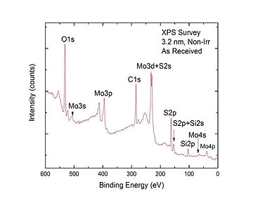
XPS Spectrum of MoS2 Thin Film
Most surfaces exposed to air contain a large fraction of O and C which must be cleaned away to begin a surface experiment.
Novel Surface Chemistry Apparatus
-
Fixed-beam AES
-
Specimen heating and cooling (77K < T < 1000C)
-
Electron Stimulated Desorption (ESD)
-
Scanning Kinetic Spectroscopy (SKS)
-
Temperature Programmed Desorption (TPD)
-
Quadrupole Mass Spectroscopy (QMS)
-
Molecular Beam Surface Physics
-
Sticking Coefficients
-
UHV Metal Evaporators for Monolayer Depositions
-
Expose Nearly any Gas to any Surface at any Temperature

%20Surface.jpg)
Si(100) Surface

Propylene Molecule


Thermal Desorption Spectrum
Desorption of propylene (C3H6) from the Si(100) surface, yielding an activation energy of ~ 1.2 eV.
Dedicated XPS Instrument
(based on Kratos XSAM 800 platform)

Deconvolution of Sn3d5/2 for Sn-Cu Metal Finish
High resolution XPS acquisition allows for peak deconvolution, identifying the identity and amount of each Sn surface oxide.

Programmable Temperature Cycling Scanning Electron Microscope
(microstructure evolution of circuitry in real-time during heating and thermal cycling)


JEOL 200 KeV Scanning Transmission Electron Microscope (STEM)
(atomic-scale structure, imaging, composition, and symmetry)


Digital Optical Microscopy
(Keyence VHX-1000)


Digital Microscopy of Coated Tin Surfaces
At surface locations showing the coating stretch as tin whiskers grow underneath.
In-Situ Dynamic Wetting Capabilities Using Scanning Electron Microscopy
(observation/analysis of liquid alloy wetting and spreading in real-time)

Real-Time Capabilities and Specs
-
Cambridge SEM fitted with a BN specimen heater and high pumping speed enables specimen heating to ~ 500 C.
-
Wetting and spreading is observed while it occurs rather than after the fact.
-
Type K thermocouple allows accurate temperature measurements during wetting.
-
Video capabilities allow alloy to be viewed during melting, wetting, and spreading.
-
Molten alloy composition can be examined by EDX.


Workhorse Scanning Electron Microscope
Environmental Hitachi S-2460N w Quartz XOne EDS
(for routine analysis of materials, interfaces, and cross-sections )


AU Rutherford Backscattering Spectroscopy Facility
(with light ion channeling and ion implantation)
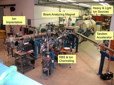
Beam-Line Configuration
-
2 million volt dual source tandem accelerator
-
Proton Irradiation: H+ @ 100 keV-4 MeV
-
Ion Implantation: Almost any ion except Noble gases 100keV-12 MeV dependent on final charge
-
Typical Elements: N, Al and P

RBS Spectrum of a Au/Pd/Ni/Cu Board Finish Used in Modern Integrated Circuits
RBS offers a nondestructive thin film analysis of layered structures used in microelectronics.
Molecular Beam Epitaxy (MBE)
(our newest big-boy toy, allowing for deposit of nanoscale thin films of high quality for microelectronics )


MBE is an epitaxial technology suited for the preparation of advanced microelectronic structures with composition and doping profiles controlled on a nanometer scale.


Flexible GaAs Solar Cell Structure Synthesized with epitaxial Ge films on metal foils: a route towards low-cost and high-performance III–V photovoltaics.
MBE System Schematically
The effusion cells generate single atom/molecule beams of metals and gases which are deposited on a substrate in an ultrahigh vacuum environment.