Research thrusts
Extreme Environment Microelectronics
We specialize in research efforts to understand the science of microelectronic materials for use in extreme environments (harsh temperatures, high pressure, high stress and strain, high radiation fields, and high vibration).
The applications are high-reliability electronics which are required to work in aerospace, space, defense, and industries using electronics in environments which cannot tolerate failure.

Pb-Free, Environmentally-Friendly, Microelectronic Materials
Until recently, there has been widespread, almost exclusive use of tin/lead (Sn/Pb) solder in the manufacture and assembly of electronic circuit boards. While Sn/Pb solder is reliable and cost-effective, environmental legislation in America, Japan, and Europe to ban or restrict the use of lead in microelectronic circuitry is of vital concern to the electronics industry. Lead is considered to be a health hazard because of the large history of human lead toxicity problems and its documented impact on human populations. Given the competitiveness of the industry and because all equipment and manufacturing requirements have been based on Sn/Pb solder, the costs of conversion to Pb-free solders and its associated reliability impacts are substantial.
The goal of our work is to develop a fundamental understanding of alternate electronic materials that will meet the high volume, high yield, and high reliability requirements for harsh environment electronics. We utilize a broad array of materials, mechanical, and thermal tests to characterize the new materials. A wetting balance allows for measurement of the adhesive forces during wetting. Video recording and heating capabilities on SEM/EDX enables in-situ, real-time observation of solder wetting characteristics. A variable-pressure, bell-jar wetting system allows studies of process gas variations on solder wetting. A high-pressure, UHV-compatible wetting chamber attached to one of our surface analysis systems allows us to study the surface physics during solder wetting and spreading. A torsion oscillating viscosity system enables measurement of solder viscosity. The oscillating sessile drop method measures solder surface tension.
A unique set of experiments has examined the behavior of the alloys during the wetting process by dynamic surface chemistry studies of the advancing liquid alloy front. Work using surface techniques such as Auger (AES) and X-ray photoelectron spectroscopy (XPS) has shown that low-level alloy impurities often segregate to the liquid surface and cause dramatic changes in wettability. One of our aims has been to determine the critical parameters that affect wetting (and materials reliability) and provide a comprehensive, atomic-scale picture of solder wetting phenomena.
In-Situ Experiments
A high-pressure and temperature cell attached to one of our UHV multi-technique surface systems, where in-situ alloy wetting under a variety of conditions can be studied.
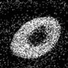
Microscopic View of Sn-3.0Ag-0.5Cu (SAC) Alloy
By scanning electron microscopy. SAC alloys offer a reasonable alternative to Sn/Pb and do not contain Pb.
Scanning Auger Map for Sn
As Sn-4.0Ag-0.5Cu wets and
spreads over a Pd surface.

Scanning Auger Map for Ag
As Sn-4.0Ag-0.5Cu wets and
spreads over a Pd surface.
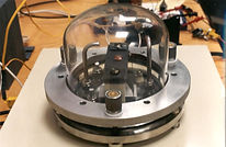
Wetting Apparatus
Custom apparatus are often needed to study surfaces. This tabletop system enables in-situ studies of solder alloy wetting.
Wide Bandgap Electronics
I'm a paragraph. Click here to add your own text and edit me. It's easy.
Heading 3
High-temperature electronic applications are presently limited to a maximum operational temperature of 225°C (435°F) for commercial integrated circuits (ICs) using silicon. One promise of silicon carbide (SiC) is high-temperature operation, although most commercial efforts have targeted high-voltage discrete devices. Depending on the technology choice, several processing challenges are involved in making ICs using SiC. Bipolar, metal oxide semiconductor field-effect transistors, and junction field-effect transistor technologies have been demonstrated at operating temperatures of up to 600°C.
"Wide bandgap" refers to electronics which is capable of operating at very high temperatures without the need for expensive cooling systems. Silicon devices fail at high temperatures because they undergo material property changes (e.g., conversion from a semiconductor to a conductor) at high temperatures and must be cooled to retain operational integrity.
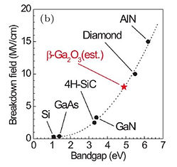
The physical and electronic properties of SiC make it the foremost semiconductor material for short wavelength optoelectronic, high temperature, radiation resistant, and high-power/high-frequency electronic devices. Collectively, these properties allow SiC devices to offer tremendous performance and reliability benefits over other available semiconductor devices in a large number of industrial and military applications.
We have been engaged in SiC high temperature electronics research for several years. The focus has been on understanding the behavior of the polar surfaces of SiC as a function of temperature, metal coverage, and gas reactivity. In addition, we have elucidated the oxidation mechanisms of SiC faces at the monolayer level, the growth modes of monolayer coverages of refractory metals on SiC, and the reactive chemistry of SiC during ohmic and Schottky barrier contact formation.
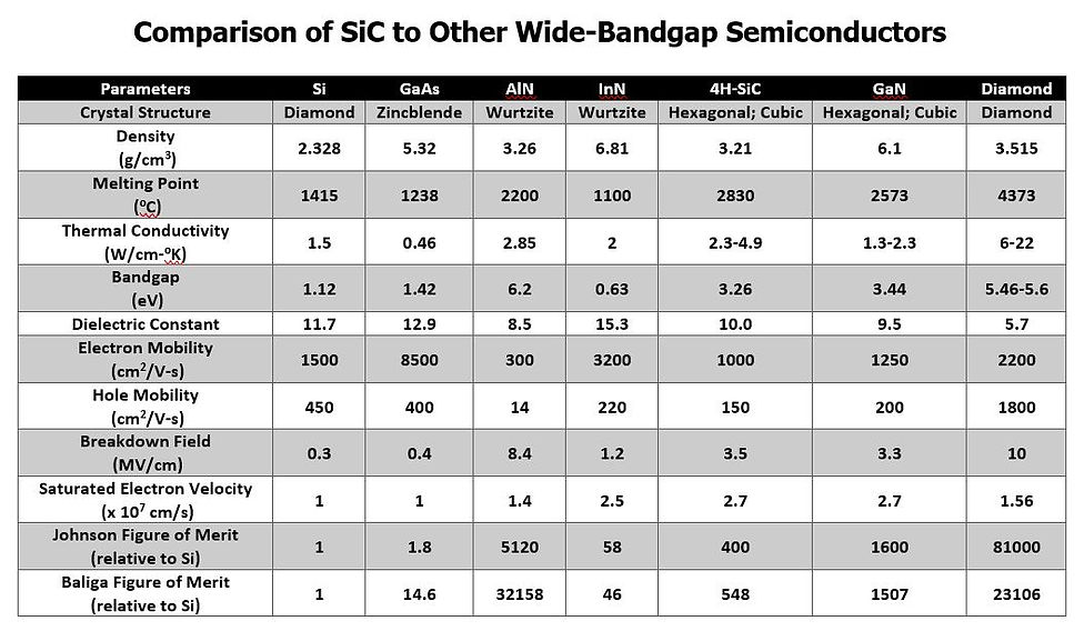
A summary of the most important properties in comparison to other wide-bandgap semiconductors . . .


Microscopic Cross-Section of a SiC-Based JFET Transistor
SiC High Voltage Power Converter
SiC Patterned Wafer


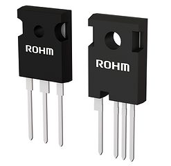
SiC Discrete Power Transistors
Some of our work on SiC surface physics . . .
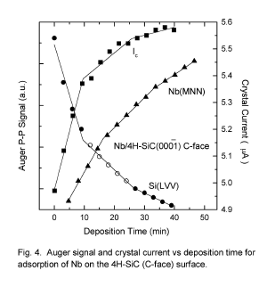
Monolayer Growth Modes of Re and Nb on the Polar Faces of 4H-SiC
K. W. Bryant and M. J. Bozack
Surface Science Laboratory, Department of Physics, Auburn University, Auburn, AL 36849 (USA)
Abstract: Auger electron spectroscopy (AES) and secondary electron emission has been used to determine how thin monolayer films of Re and Nb grow on the 4H-SiC (C-face) and 4H-SiC (Si-face) surfaces at room temperature. The secondary electron emission was monitored by the crystal current (SEECC) method and compared to the change in Auger electron peak-to-peak intensities for both substrate and adsorbate. On the 4H-SiC (Si-face), both metals first form a single monolayer followed by growth of simultaneous monolayers (MSM mode). On the 4H-SiC (C-face), both metals grow layer-by-layer (Frank-van der Merwe, FM mode).
Surface Composition of 4H-SiC as a Function of Temperature
K. W. Bryant and M. J. Bozack
Surface Science Laboratory, Department of Physics, Auburn University, Auburn, AL 36849 (USA)
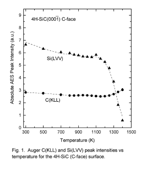
Abstract: We report surface compositions of the 4H-SiC(C-face) and 4H-SiC (Si-face) over the temperature range 300 to 1400 K, studied by Auger electron spectroscopy (AES), energy loss spectroscopy (ELS) and quadrupole mass spectroscopy (QMS). Below 800 K, no significant changes in surface composition are observed. Between 800 K and 1200 K, silicon preferentially volatilizes, leaving a slightly graphitized surface. Above 1200 K, preferential volatility of silicon results in a heavily graphitized surface. The thickness of the graphitized layer is greatest on the 4H-SiC(C-face) surface (~ 8 Å @ 1400 K). Results are compared with earlier work involving the polar faces of 6H-SiC.